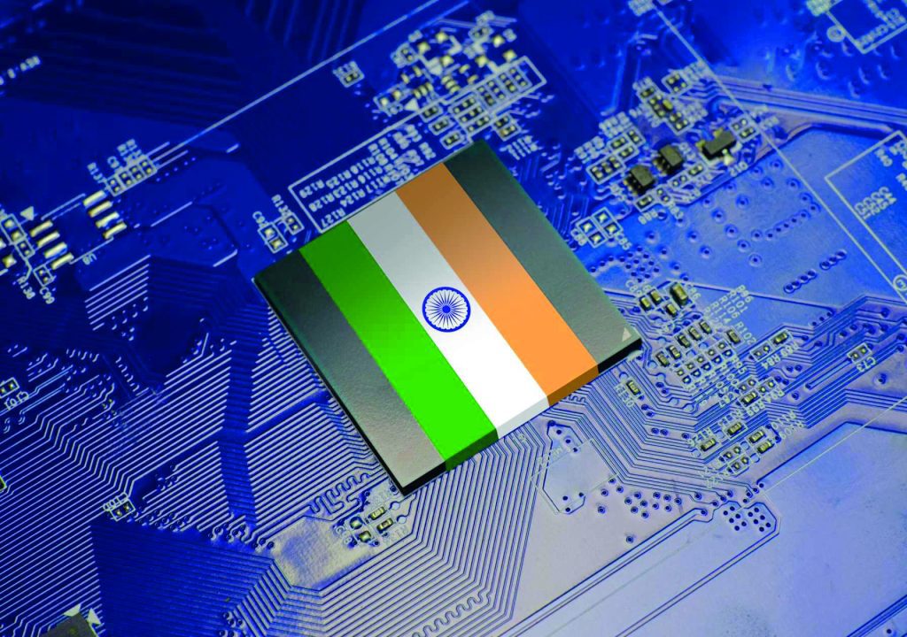
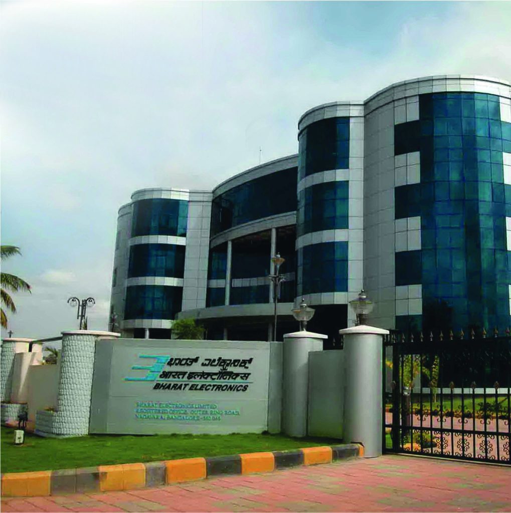
Semiconductors are ubiquitous with their requirement in wide ranging sectors covering consumer electronics, automobiles, strategic sectors, biomedical equipment, among others. Semiconductors have thus emerged as a very important sector for the growth of any nation. Essentially, semiconductor microchips as Integrated Circuits (ICs), primarily made out of silicon, are used to fabricate electronic devices. From as early as the 1960s, there were several attempts by the Indian government as well as private individuals and industries to set up semiconductor fabrication facilities in the country. Being a capital intensive industry, previous attempts did not materialise. There are facilities at Bharat Electronics Limited, Bengaluru; Semiconductor Complex Limited, Chandigarh; GATECH, Hyderabad, among others within the country.
However, with ambitious economic goals, India needs to support its fast growing as well as established industries like automobile, biomedical equipment, consumer electronics, and strategic sectors. Among consumer electronics, most visible are the smart televisions and mobile phones which are mostly assembled in India. To make them more affordable and save on foreign exchange, it would be ideal to have manufacturing facilities for semiconductor chips as well as display units within India. Instead of contract manufacturing for multinationals, the value addition comes in having design capabilities within the country.

The Covid-19 Impact
Most notable changes in recent history happened during the Covid-19 pandemic. The change in lifestyle necessitated by the pandemic, for example, required more electronic gadgets for communication, and less use of automobiles. While the lockdowns affected the supply chains and shortage of chips, they also resulted in an increased demand for electronic gadgets. The after effects are still seen, particularly, in the automobile, high-end scientific equipment, and strategic sectors. Further demand for semiconductors is expected only to increase in the coming years. Pandemic disruptions and geopolitical tensions highlighted the need for a self-reliant India. The government of India launched the Indian Semiconductor Mission (ISM) in June 2021 aiming to strengthen the semiconductor industry by attracting global semiconductor companies through its policies, incentives, and investment. Despite the past setbacks, India is putting its best efforts now to promote domestic chip manufacturing units, display units, compound semiconductors, and design infrastructure.
This mission is not only expected to contribute to India’s growth but also significantly to the global electronics value chain. The present demand for semiconductors in India of around $24 billion is entirely met through imports and is expected to reach $100 billion by 2025. The growth of the semiconductor sector is primarily driven by increasing semiconductor content in consumer electronics, automobiles, including electric vehicles, the adoption of 5G and IoT devices. This is expected to grow further for emerging applications with more chip content needed for automation in automobiles, autonomous machines, smart medical devices, 6G communications, AI, and unmanned aerial vehicles. Thus, ISM is an appreciable move towards self-reliance.

Science & Technology behind Semiconductors
Semiconductors are widely used in everyday life now with the penetration of mobile phones, computers, digital cameras, televisions, washing machines, refrigerators, lighting including LED bulbs, sensors, and automobiles to name a few. Strategic sectors like space, defense, wireless communication are also being advanced by semiconductors. Logic devices play a critical role in novel appliances based on artificial intelligence.
Semiconductors are materials with electrical conductivity that can be freely controlled by one means or the other. These have an electrical resistance inbetween that of conductors (metals) and insulators (for example, ceramics). The elemental semiconductors are those composed of single species of atoms, such as Silicon (Si), Germanium (Ge), Tin (Sn), Selenium (Se), Cadmium (Cd), Tellurium (Te), etc. Extrinsic semiconductors are prepared by adding a small amount of impurity or doping. When a trivalent impurity like Indium (In), Gallium (Ga), Aluminum (Al), or Boron (B) is added, the semiconductor becomes p-type having electron deficiency. On the other hand, an n-type semiconductor having excess electrons can be realized by adding a pentavalent impurity like Arsenic (As), Antimony (Sb), Phosphorous (P) and Bismuth (Bi, elements having five valence electrons). There are compound semiconductors as well, such as Gallium Arsenide (GaAS) or Cadmium Selenide (CdSe) which are realized by mixing group III and group V elements from the periodic table. There are several advantages and applications of compound semiconductors in power electronics, optoelectronics, high speed electronics, among others. Diamond is another wide bandgap semiconductor that finds applications in high-power electronic devices due to its exceptional properties. Diamond’s dielectric breakdown strength is three times higher than silicon carbide (SiC) and more than 30 times higher than silicon (Si). In addition to silicon which will cater to general requirements, compound semiconductors and diamond used in niche applications need to be considered.
Among the semiconductor devices, a diode is the most basic one that acts as a one-way switch allowing current flow in only one direction. A diode is having a junction between p and n layers. In 1874, Karl Braun discovered that current flows freely in only one direction at the contact between a metal point and a galena crystal. Subsequently, a crystal detector for radio waves was patented by Jagadish Chandra Bose in 1901. Transistor is another commonly used semiconductor device that was invented at Bell Labs, USA, in 1947. It is a three layer and 3 terminal device that regulates current or voltage flow in a circuit. Transistor is also used for amplifying and generating electrical signals as well as for switching/gating. There are several types of transistors and other devices that are constituents of present day compact, reliable, efficient and economical chips for micro-electronics/VLSI, displays, solar cell devices, etc.
The number of transistors on a chip doubled almost every 1.5 years over the last many decades pushing the fabrication technology requirements to their limits. There is continuous innovation at select companies like ASML, Netherlands, to make the needed fabrication systems. This partially makes semiconductors a cost-intensive industry which requires sophisticated fabrication or lithography tools that cost about 10s of million dollars each.
How can India become a Semiconductor hub for the world?
The recent global chip shortage and geopolitical factors drive the need for alternate semiconductor manufacturing hubs in the world. The government of India initiated work towards atmanirbharta / self-sufficiency in semiconductors by launching the ISM in 2021 to establish the ecosystem for electronics manufacturing. This mission aims to enable India’s emergence as a global hub for electronics manufacturing and design with a financial outlay of INR 76,000 crore. The mission is a long-term strategy for developing semiconductor manufacturing facilities and semiconductor design ecosystem in the country. The government has framed ISM in consultation with ministries / departments / agencies, industry, and academia. Further, to provide requisite support for the supply chain, Electronic Design Automation (EDA) tools, foundry services and other suitable mechanisms for early-stage start-ups are included in the semiconductor mission. Under this mission, four schemes have been introduced, namely, (i) setting up of semiconductor fabs (ii) display fabs (iii) compound semiconductor/silicon photonics/sensors fab and (iv) semiconductor assembly/testing, marking and packaging. Scheme also includes outsourced semiconductor assembly and test (OSAT) facilities in India.
The government is leaving no stone unturned and looking resolute to provide adequate infrastructure, expertise, and resources to make the mission successful. To facilitate semiconductor production in the country, the Indian government has included several impressive initiatives such as the production-linked incentive (PLI) and design-linked incentive (DLI) schemes to support companies for setting up semiconductor manufacturing facilities in India. Further incentives such as tax breaks, and eased regulations are offered to attract more investments in the semiconductor sector. In addition, we need to ensure constant feed into the semiconductor supply chain, including raw materials, specialty chemicals, gases, and manufacturing equipment. Through ISM, the government is anticipating establishing a reliable semiconductor-based microelectronics supply chain, including indigenous intellectual property generation, transfer of technologies, and collaborations with international organisations to promote research and commercialisation.
Presently, a significant portion of the value chain is located in three major countries, Taiwan, South Korea and China and to some extent in the USA, Japan and the Netherlands. Taiwan alone produces sixty percent of the world’s total semiconductor chips. The US, through its CHIPS act, also wants to boost semiconductor manufacturing in the country for its own economy with the aim to combat China’s chip-making hub. In the recent past, it is seen that Germany is also emerging as a producer of semiconductor chips. All these countries have established themselves as semiconductor manufacturing hubs and thus may offer stiff competition to India.
In spite of this, the global community has welcomed the government’s move to encourage semiconductor manufacturing in India, with India and USA signing an agreement to collaborate on this issue. Semiconductors, which have been a key strategic focus for both India and the US, featured in the talks between Prime Minister Narendra Modi and the US President Joe Biden, during the former’s visit to the US in June this year. The leaders had reiterated their support for building a resilient global semiconductor supply chain. While, Microchip Technology, Inc has proposed to invest approximately US$300 million in expanding its research and development presence in India, Advanced Micro Device announced plans to invest US$400 million in India over the next five years to expand research, development, and engineering operations in India’.
Some are already complaining about the second call from GoI, for proposals to set up facilities in India, as a delay in the implementation of the mission. However, India needs to take lessons from past experience in setting up, operating, and making high end chips and equipment within India at places like Semiconductor Complex, and GATECH, as well as from our past attempts at bringing semiconductor majors to India.
At the outset, we need to acknowledge that it takes time and resources to build a complete value chain in India for semiconductors. Setting up of semiconductor manufacturing plants requires not only significant infrastructure such as power, water, high-grade chemicals (often referred to as electronic or semiconductor grade chemicals) and transportation facilities but also expertise in design and fabrication through highly skilled manpower. These require incentives to develop the local value chain including production of silicon wafers, and training of manpower. The value addition to the industry is by way of designing high end electronic chips locally and fabricating them. This will help industry gradually evolve and progress with all kinds of materials, processes, and technologies required for semiconductor chips.
One notable area where India may lead is in carbon neutrality. Semiconductor process facilities generate toxic chemicals, gases and hazardous waste which require safe disposal. Further, the majority of wafer fabrication facilities around the world are operational without much thought of sustainability. As India is embarking on its long journey, through its semiconductor mission, it can also lead the way by keeping in sight the carbon neutral targets promised by the government. Meeting the power requirements through renewable energy sources, safe disposal of toxic waste, use of recycled water and chemicals, and use of green materials in semiconductor processing could help reduce the carbon footprint of these facilities. If India creates silicon growth and chip fabrication facilities having low carbon footprint and less capital-intensive technologies (as ISRO has done in space technology), it can show the world the viability of sustainable semiconductor manufacturing. This can also encourage the rest of the world to move to India as a global semiconductor hub for their requirements. In addition, India needs to focus on indigenous content in the areas of Artificial Intelligence (AI), Internet of Things (IoT), and robotics in semiconductor chip fabrication facilities in India. This will help in reduction of processing cost and may tide over any natural or geopolitical disruptions. Adoption of circular economy practices into future semiconductor chip manufacturing would help align with the UN Sustainable Development Goals (SDGs).
If India is looking to reach the ambitious economic goals set by the government to be reached by 2047, then ‘make in India’ electronic chips to complex systems will significantly add to the overall GDP of the country. Towards this, the development of a sustainable semiconductor and display ecosystem in India is essential.
The success of the mission will depend upon how much India accomplishes its set goals towards attracting semiconductor companies to invest in the country. However, there are several reasons to believe in the success of ISM. MoU with the USA is beneficial for both countries in their semiconductor programs. In addition to the US majors Micron Technology and Applied Materials, Taiwan Semiconductor Manufacturing Company (TSMC), Taiwan, has also shown interest in establishing a semiconductor manufacturing hub in India.
In view of the progress that has happened since the launch of ISM, it looks quite certain that in the coming years, the efforts of the government will make India compete in the global semiconductor chip making race. Semiconductors designed and developed for the next phase of digital transformation under Industry 5.0 with green technologies having a low carbon footprint are to be adopted. Sustainability could be the hallmark of the Indian competency in semiconductor manufacturing, which may set the course for the rest of the world. Indian trade policies coupled with net-zero carbon goals and Indian Semiconductor Mission will certainly build an ecosystem for electronic chip manufacturing in the country.
*Dr Sushil Kumar is Chief Scientist, CSIR-NPL and Prof Venu Gopal Achanta is Director, CSIR-NPL.


